

ARM Architecture with Each Module’s Working Principle


The ARM microcontroller stands for Advance RISC Machine
These processors are specifically used in portable devices like digital cameras, mobile phones, home networking modules and wireless communication technologies and other embedded systems due to the benefits, such as low power consumption, reasonable performance, etc.
ARM Architecture
The ARM architecture processor is an advanced reduced instruction set computing [RISC] machine and it’s a 32bit reduced instruction set computer (RISC) microcontroller
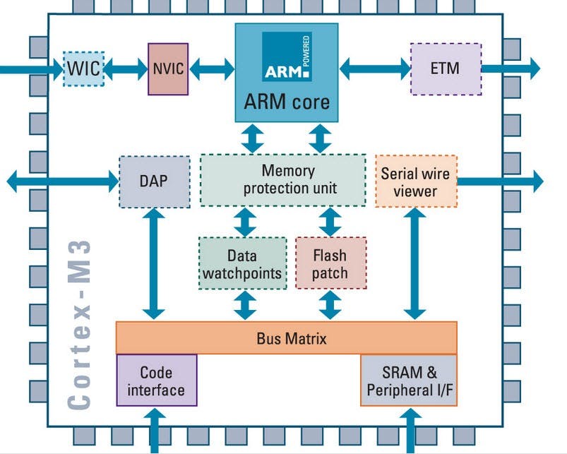
The ARM cortex is a complicated microcontroller within the ARM family that has ARMv7 design. There are 3 subfamilies within the ARM cortex family :
- ARM Cortex Ax-series
- ARM-Cortex Rx-series
- ARM-Cortex Mx-series
The ARM Architecture
- Arithmetic Logic Unit
- Booth multiplier
- Barrel shifter
- Control unit
- Register file
The ARM processor conjointly has other components like the Program status register, which contains the processor flags (Z, S, V and C). The modes bits conjointly exist within the program standing register, in addition to the interrupt and quick interrupt disable bits; Some special registers: Some registers are used like the instruction, memory data read and write registers and memory address register.
Priority encoder: The encoder is used in the multiple load and store instruction to point which register within the register file to be loaded or kept .
Multiplexers: several multiplexers are accustomed to the management operation of the processor buses. Because of the restricted project time, we tend to implement these components in a very behavioral model. Each component is described with an entity. Every entity has its own architecture, which can be optimized for certain necessities depending on its application. This creates the design easier to construct and maintain.
Arithmetic Logic Unit (ALU):
The ALU has two 32-bits inputs. The primary comes from the register file, whereas the other comes from the shifter. Status registers flags modified by the ALU outputs. The V-bit output goes to the V flag as well as the Count goes to the C flag. Whereas the foremost significant bit really represents the S flag, the ALU output operation is done by NORed to get the Z flag. The ALU has a 4-bit function bus that permits up to 16 opcode to be implemented.
Booth Multiplier Factor:
The multiplier factor has 3 32-bit inputs and the inputs return from the register file. The multiplier output is barely 32-Least Significant Bits of the merchandise. The entity representation of the multiplier factor is shown in the above block diagram. The multiplication starts whenever the beginning 04 input goes active. Fin of the output goes high when finishing.
Booth Algorithm:
Booth algorithm is a noteworthy multiplication algorithmic rule for 2’s complement numbers. This treats positive and negative numbers uniformly. Moreover, the runs of 0’s or 1’s within the multiplier factor are skipped over without any addition or subtraction being performed, thereby creating possible quicker multiplication. The figure shows the simulation results for the multiplier test bench. It’s clear that the multiplication finishes only in16 clock cycle.
Barrel Shifter:
The barrel shifter features a 32-bit input to be shifted. This input is coming back from the register file or it might be immediate data. The shifter has different control inputs coming back from the instruction register. The Shift field within the instruction controls the operation of the barrel shifter. This field indicates the kind of shift to be performed (logical left or right, arithmetic right or rotate right). The quantity by which the register ought to be shifted is contained in an immediate field within the instruction or it might be the lower 6 bits of a register within the register file.
Control Unit:
For any microprocessor, control unit is the heart of the whole process and it is responsible for the system operation,so the control unit design is the most important part within the whole design. The control unit is sometimes a pure combinational circuit design. Here, the control unit is implemented by easy state machine. The processor timing is additionally included within the control unit. Signals from the control unit are connected to each component within the processor to supervise its operation.
ARM7 Functional Diagram
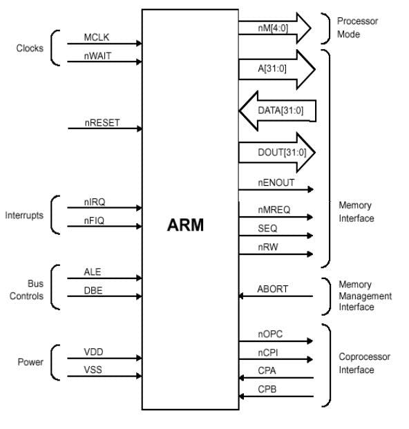
The final thing that must be explained is how the ARM will be used and the way in which the chip appear. The various signals that interface with the processor are input, output or supervisory signals which will be used to control the ARM operation.